A technique for designing two-dimensional films that can fold into three-dimensional microsurfaces could be used in new tech, such as artificial retinas.
The art of folding two-dimensional paper into beautiful three-dimensional shapes is more than a thousand years old. And while its exact place of origin in eastern Asia is unclear, today it’s most readily associated with the Japanese word origami. One modern challenge is how to make these kinds of folds at the microscale, which would enable the construction of tiny devices for use in biomedical technology, batteries, and catalysis.
Yihui Zhang from Tsinghua University and his colleagues have developed innovative new microlattice design models for transforming two-dimensional thin films into three-dimensional curved surfaces.
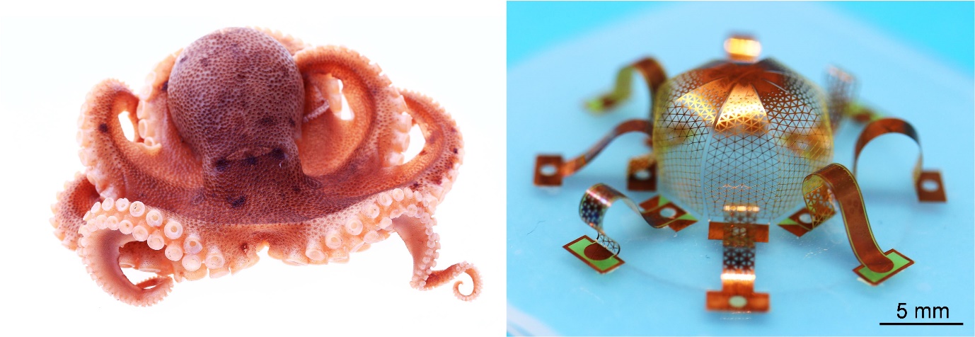
Tsinghua researchers used microlattice designs to create a 2D template that could be folded into this millimeter-scale octopus.
Their findings were recently published in the prestigious journal Science.1 In the equally impactful journal Nature, which reported on the study, a writer points out that the bioinspired microlattice strategy “could be harnessed to build structures out of materials ranging from silicon to polymers to graphene”.2
Some types of silicon have been particularly difficult to shape due to their brittleness, Zhang points out. His work will be particularly useful when applied to these difficult materials.
In 2016, Zhang was recognized by the MIT Technology Review as one of the world’s leading innovators under the age of 35 for his work on mechanically-guided assembly of 3D nanoscale structures.
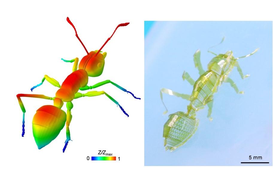
A Tsinghua team designed this ant, which is formed from more than 4,000 microtriangles and almost 8,000 microribbons.
Inspirations from natural geometry
It’s sometimes difficult to flatten a curved surface into a plane without stretching or tearing parts, says Zhang. A globe of the world, for example, cannot be transformed into a two-dimensional map without serious distortions of its shape and the relative sizes of many countries. In the case of materials, such nonuniform stretching would cause changes in the atomic structure, altering the substance’s mechanical and electronic properties. These are called ‘undevelopable’ curved surfaces.
A solution is to divide the curved shape into a lattice of flat discrete elements, a concept known as ‘discretization’. This idea can be seen in geometric glass domes made from lattices of triangular panes. But as the three-dimensional shape becomes more complicated, the two-dimensional discretized lattice must also become more elaborate.
So, the problem then becomes how to design a two-dimensional lattice for complex curved, three-dimensional microstructures. By taking the inspiration from microlattices found in nature, Zhang and his co-workers used analytical and computational modeling methods to design both artificial and natural 3D shapes or ‘mesosurfaces’ starting from a flat surface.
“Learning from nature is important for materials science, because nature has evolved over millions of years to create materials that are optimized for their specific functions,” explains Zhang. The natural world is full of examples of microlattices with complex 3D layouts, he says. To give just one example, lattices made up of vascular networks in cabbage leaves locally shrink and thicken at low temperatures to form a cabbage’s multilayer spherical shape.
Shaping new devices
The team applied their microlattice design strategy to a wide range of materials, including metals, laser-induced graphene, chitosan (a material found in the exoskeletons of insects and crustaceans) and even a brittle form of monocrystalline silicon, which had previously thought to be impossible to shape owing to its fragility.
They were able to create more than thirty different structures with different shapes with lateral lengths ranging from ~ 0.25 to 30 millimeters.
“The octopus-shaped and the ant-shaped microsurfaces are my favorite 3D structures from this work,” Zhang says. “They truly look like the real objects, while their complex shapes demonstrate the powerful capabilities of our microlattice-based shape programming methods.”
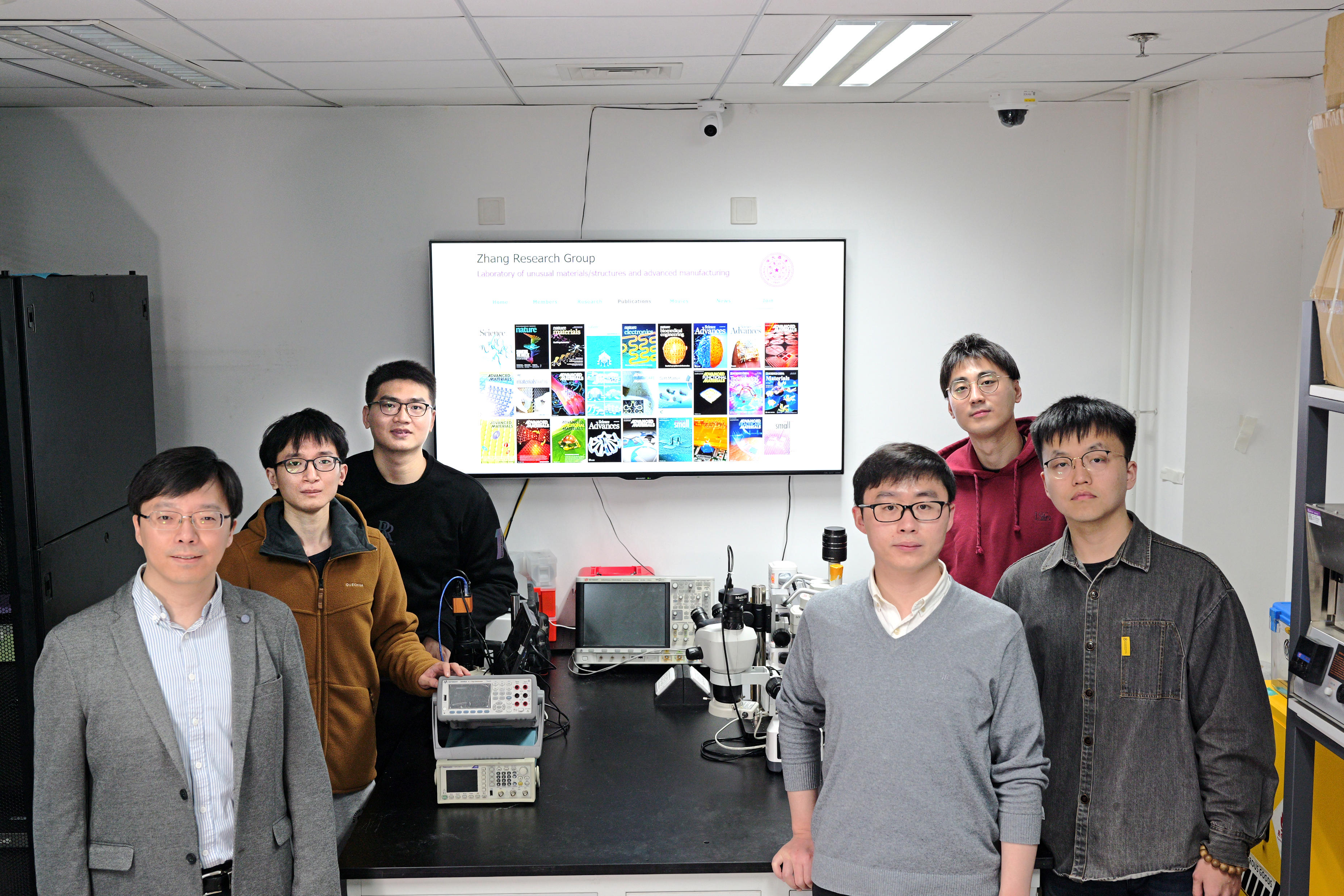
Yihui Zhang (at left) and his team from Tsinghua University’s Applied Mechanics Laboratory and Laboratory of Flexible Electronics Technology.
The next possible step in this research is to combine biocompatible materials (e.g. the chitosan) with a high density of sensing electrodes. The ultimate goal, says Zhang, is to develop biomimetic robotics and biocompatible devices, such as implantable artificial retinas “that are capable of providing high-resolution imaging by detecting and processing signals from living retinal cells”.
Zhang’s study was done with colleagues from Tsinghua University’s Applied Mechanics Laboratory and Laboratory of Flexible Electronics Technology, along with researchers from Hunan University and the University of Science and Technology Beijing, in China, and Northwestern University in the United States.
References
1. Cheng, X., Fan, Z., Yao, S., Jin, T., Lv, Z. et al. Programming 3D curved mesosurfaces using microlattice designs Science 379, 1225–1232 (2023) doi: 10.1126/science.adf3824
2. ‘Life’s wondrous forms recreated in graphene and more’ Accessed on 5 November 2023 at https://www.nature.com/articles/d41586-023-00878-5 doi: 10.1038/d41586-023-00878-5
Editor: Guo Lili