Three-dimensional (3D) printing represents the cutting-edge manufacturing approach as it revolutionizes designs and traditional manufacturing techniques, such as casting, coating, photolithography, and nano-imprinting. For instance, through programming laser scanning paths in 3D, materials can be constructed into arbitrary 3D nanostructures – this process is also known as laser 3D nanoprinting. It provides the possibility of fabricating nanoscale devices with fascinating functionalities that do not occur in nature, such as the negative refractive index, artificial chirality, ultralight mechanics, and so on. However, existing laser printing techniques typically require polymer-nanomaterial composites and are limited by the photopolymerization mechanism, resulting in a reduction of material purity and the degradation of intrinsic properties.
To address this technical challenge, Hong-Bo Sun, Linhan Lin and their research team from the Department of Precision Instrument at Tsinghua University have developed a new laser nanoprinting technique termed photoexcitation-induced chemical bonding (PEB), which is capable of organizing diverse nanomaterials into arbitrary 3D structures. PEB does not require any polymer additives or special designs of precursors and can directly assemble nanomaterials in free spaces with light, with a minimum printing linewidth of just 77 nm. This work has been published in the latest issue of the journal Science.
“We were deeply attracted by this experimental phenomenon from the first time we observed it,” Lin said. “Under laser illumination, nanomaterials were excited and further connected to each other to form structures in an unexpected way.”
To reveal the underlying mechanism, Liu and Hou (the lead authors of this work) have conducted a series of controlled experiments and confirmed that the high-energy carriers, through photoexcitation, play a significant role in initiating the printing process. Under photoexcitation, the holes excited inside quantum dots are transferred to the nanocrystal surface and improve their chemical reactivity, leading to interparticle chemical bonding (Fig. 1).
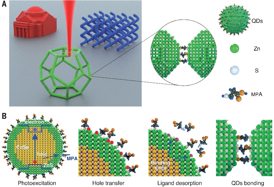
Fig. 1 Working principle of PEB
As a proof-of-concept, researchers have successfully realized the 3D printing of nanomaterials into a wide range of complex structures, ranging from linear and curved to volumetric nanostructures at high resolution and high accuracy (Fig. 2). The heterogeneous integration of multi-materials in single structures was also achieved for multi-color 3D display. This technique paves the way in the fabrication of multifunctional optoelectronic devices, such as quantum dot light-emitting diodes or photodetectors.
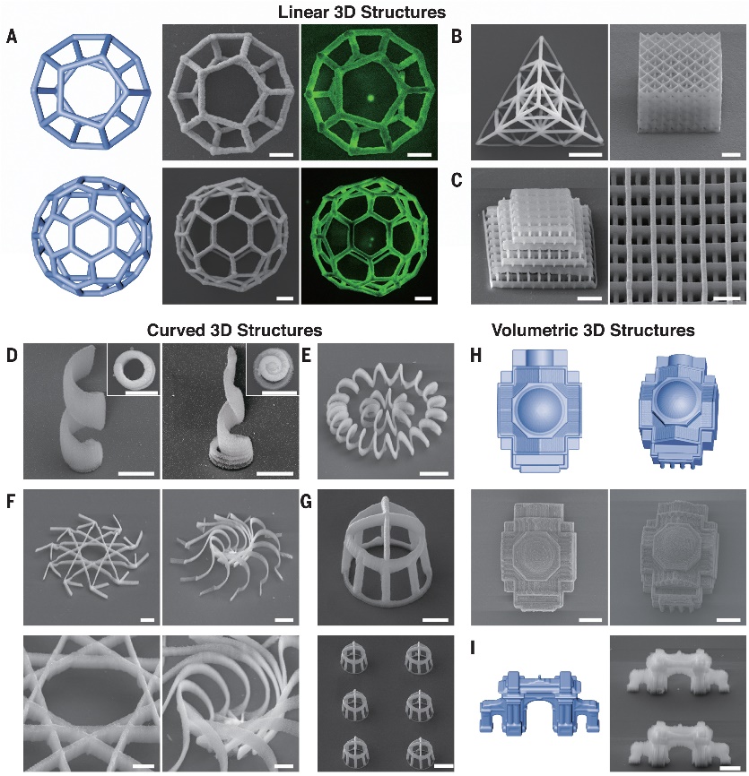
Fig. 2 Linear, curved, and volumetric 3D nanostructures
“Using various nanocrystals synthesized chemically as building blocks, we expect to build integrated functional nanodevices that cannot be built using traditional techniques”, Sun concludes, “It will break the existing design rules and facilitate the development of new-concept nanophotonic or optoelectronic devices”.
This work was supported by the National Key Research and Development Program of China, the National Natural Science Foundation of China, the Tsinghua-Foshan Innovation Special Fund, and the State Key Laboratory of Precision Measurement Technology and Instruments.
Original Article Link: https://www.science.org/doi/10.1126/science.abo5345
Editor: Li Han